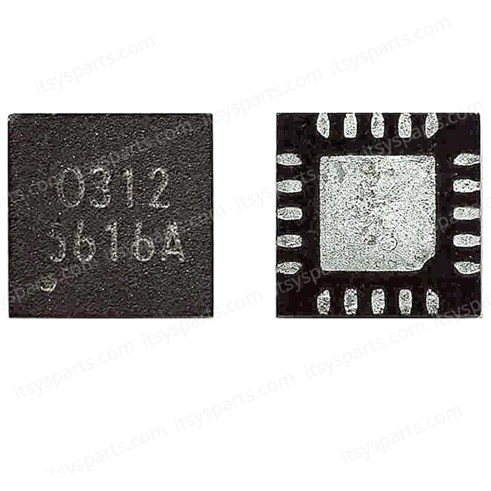
- Stock: In Stock
- Brand: Unbranded
- Model: 1-CHIP0456
- SKU: 1-CHIP0456
Realtime Stock
Controller IC Chip - MOSFET G5616ARZ1U G5616A 5616A G5616 QFN20 chip for laptop- Integrated portable calculator chip(SKU.1-CHIP0456)
Complete DDR, DDRII and DDRIII Memory Solution Synchronous Buck PWM Controller, 3A LDO, Buffered Reference
The G5616 is intended for DDR/SSTL-2, D-DRII/SSTL-18 and DDRIII memory systems. It inte-grates a synchronous buck PWM controller with a 3-A sink-source linear regulator and buffered reference. The PWM controller uses constant on-time control scheme to handle wide input/output voltage ratios with ease and provides 100ns “instant-on†response to load transients while maintaining a relatively constant switching frequency. The G5616 achieves high effi-ciency at a reduced cost by eliminating the cur-rent-sense resistor found in traditional current-mode PWMs. Efficiency is further enhanced by an ability to drive very large synchronous rectifier MOSFETs. Sin-gle-stage buck conversion allows these devices to directly step down high-voltage batteries for the high-est possible efficiency. The 3A sink/source tracking termination regulator is specifically designed for low-cost/ low-external com-ponent count systems. The regulator contains a high speed operational amplifier that provides fast load transient response with only 20mF (2x10mF) of ceramic output capacitance. The G5616 supports remote sensing functions and all features required to power the DDR /DDRII /DDRIII VTT bus termination accord-ing to the JEDEC specification. In addition, the G5616 includes integrated sleep-state controls placing VTT in High-Z in S3 (suspend to RAM) and soft-off for VTT and VTTREF in S5 (Shutdown). The G5616 provides OVP, UVP, over current and thermal shutdown protection functions and is available in a 20-pin 3X3 TQFN package and 24-pin 4X4 TQFN includes over voltage protection.
•Synchronous Buck Controller (VDDQ)„Ultra-High Efficiency „No Current-Sense Resistor (Lossless ILIMIT) „Quasi-PWM with 100ns Load-Step Response „1.8V(DDRII) /1.5V(DDRIII) Fixed or Adjustable to 2.5V(DDR) or 0.75V to 3.6V Adjustable Out-put Range „2V to 24V Battery Input Range „400kHz Switching Frequency „OVP & UVP of VDDQ Output „Drives Large Synchronous-Rectifier FETs „Power-Good Indicator•3-A LDO (VTT), Buffered Reference (VTTREF)„Support DDR (1.25 VTT) , DDR II (0.9 VTT) and DDRIII(0.75 VTT) Requirements „VLDOIN Voltage Range: 1.2V to 3.6V „Requires Only 20mF Ceramic VTT Output Ca-pacitance „Supports High-Z in S3 and Soft-Off in S5 „Integrated Divider Tracks 1/2 VDDQSNS for Both VTT and VTTREF „Remote Sensing (VTTSNS) „±20mV Accuracy for VTT and VTTREF „10mA Buffered Reference (VTTREF) „Built-In Soft-Start to Reduce the VLDOIN Surg-ing Current „Over Current Protection of VTT Output „Thermal Shutdown Protection
Please check the IC Number and match with your existing Product.
When you receive before using it.
Please confirm the chip you received is brand new as described,if you suspect the chip is not new or not as described. Please don't use it and contact us immediately.
Please make sure you have advanced soldering skill to solder the chips that you will order.
Once it has been used, no return will be accepted.


